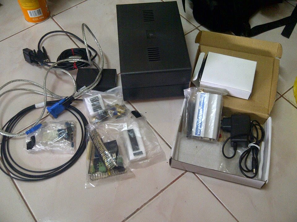
Friday, April 4, 2014

Final Year Project2 (Hardware) Week8

Title: Create the real PCB to make a virtual circuit

Objectives:

  • Recheck all the PCB layout 
  • To create the virtual circuit for Microcontroller circuit and relay circuit
Procedure:

  • List all the component that are involved in this session. The component were:
PCB(fibre),masking tape,transparent paper PCB

PCB pen

acid etching
  • The PCB (fibre) needed to be printed by using the transparent paper as shown in figure below:
          This step are using the iron to heat up the transparent paper that have printed with the circuit                          MicroController diagram. 

After iron the transparent paper
  • The circuit diagram that are appear at the PCB fiber are not cleared enough, so it must be touch up by using the PCB pen as shown as figure below:
Cleared PCB printed
  • After that, the PCB must be included the etching processes. The purpose of this processed are to remove the unwanted copper to create a circuit diagram. This step are using the etching acid and hot water. Just shown as Figure below:
Step1: put the etching powder into the plastic bowl

Step2: Put boiled water to the etching powder

Step3: Put the PCB into the bowl

Step4: Etching process end

  • The PCB are settled with etching processed. Next, needs to clean up the black ink color at the top of the copper circuit line:

After cleaning
  • Drilling process are required to put the component into the PCB:

Drilling process
Put component to PCB


Result and Analysis:
  • The PCB for MicroController are designed well. All component such as PIC16F887,Crystal 20Mhz,connector,resistor,voltage regulator 7805,capacitor 22pF and resistor 1K & 47K.
  • The component needs to be solder so that the component will conduct electricity very well.


Conclusion:
  • The PCB for Microcontroller circuit are designed well. Next, it will be tested after all the component are ready enough to put into the PCB. 
  • LCD 16x2 needs to be solder properly to connected into this board.
  • Next, etching the relay circuit and tested both circuit.


Thursday, March 27, 2014

Final Year Project2(Hardware) Week7

Title: Find suitable car model

Objectives:

  • To find a car model that are suitable and can be used into my final year project
  • The car model must be at least width=6 inch,length =16inch and high=6 inch
  • the car model must can be fit in the main controller circuit and relay circuit
Procedure:
  • Go to the supermarket and find the car model that cannot function well with the cheaper price because the purpose of finding this car model are only wants to get their body and chassis not the circuit for the controlling the car.
Microcontroller circuit fit to the model

car model satisfy the specification
  • After the car model that satisfy the objectives, next the chassis needs to do some modification to create the 4 door system that can react as real door simulation for a car.
step1

step2

step3

step4
  • For the Step1, Draft the pattern for real door car to make it possible to open
  • Step2, after draft by using marker, the image of the 4 door are clear already. So, cut the door that followed the line that has been created before this and separated it from plastic chassis.
  • The plastic chassis are thin and not strong enough to hold the pressure and load from human hand. So, it must be redesign by using the cardboard paper that are more thick and strong enough to hold the pressure as shown at step3.
  • Step4 are shown about the design that are created at cardboard paper that can opened the car doors.
  • after Step4, the door that had been cut before this needs to put a gum and to make sure the door are hard enough to hold the human hand pressure.

Result and Analysis:

  • The car model are satisfy the objectives of this week because the 4 door can be opened and the car model can open and close the door properly by some modification.
  • The importance to find the right car model is to make sure that the car are exactly could be same as real car viewer.
Conclusion:

  • The objectives for finding the car model are acheive and the door can be well opened, same as the virtual car system that are simply can tell people about this project purpose due to the real situation while the thief wants to opened the car doors.

Friday, March 21, 2014

Final Year Project 2(Hardware) Week6

Title: Build and test the main circuit (Microcontroller) at bread board

Objectives:

  • To construct and tested the main circuit(Microcontroller) at bread board
  • To make make sure the coding that been burned at Microcontroller PIC16F887 are fully working
Procedure:
  • Construct the circuit at bread board by referring circuit from the Proteus simulation before this
Proteus simulation for main circuit
Main Circuit are constructed
  • After the circuit are constructed, the circuit are been tested as shown above.
Result and Analysis:
  • For the first circuit construct, there is a problem regarding the connection. The LCD 16x2 are didn't display the output due to the failure of the supposed connection.

LCD failure

  • After troubleshoot the lcd, connection are successfully done and the problem are solved
  • According the simulation, 1st the LCD will display 'READY'


  • Then, it will display 'GSM Security Car'


  • When the PB2 is pressed, it will turn on the switch that will located at door car panel, there's 4 switch that connected parallel just like the proteus simulation shown. 

PB2 pressed
The LCD will display 'System On' just after the PB2 is pressed


  • After 'System On' it will activated the Door Switches that connected at parallel line. The working scheme for the Door Switches are working when there's one of the switches turn on, the LCD will display 'Sending Message' which means the MicroController will sending message to the GSM system, than the LCD will display 'Warning' that will alerted people that try to stole the car.
  • Actually, after the LCD are display 'Sending Message' and 'Warning', the Relay 5vdc will react to cut-off the supply for the Ignition System of the car. But in this testing, the Relay part are not included because of the relay and GSM circuit are build separated from the Main circuit. The Relay 5vdc and GSM will be tested after this session.

Conclusion

  • The coding that are burned for the PIC16F887(Microcontroller) are successfully done perfect but after some kind of troubleshoot because of failure to do a correct wiring and some short circuit are produced that caused the Microcontroller cannot perform well.
  • It is important to test the main circuit at the bread board to check weather the coding that are burned at Microcontroller are perfectly perform or not.
  • After the circuit at bread board are perform well, it will build a confidence level to create a PCB circuit according to the PCB layout that are created by using PCB Wizard before this.

Friday, March 14, 2014

Final Year Project 2(Hardware) Week5


Title: Readjustment the PCB layout

Objectives:

  • To make sure that the PCB layout design are suitable with the virtual circuit
  • To compromise with the supervisor about the PCB layout design 
  • But the component part to build a virtual circuit
Procedure:


  • Open the  PCB Wizard software that contain the previous PCB design and rebuild it to make it more compatible and alternate with the virtual circuit. 

Previous PCB design

  • From Proteus software, list down all the electronic component that needs to buy at Jalan Pasar
Result and Analysis:

  • New PCB design for Microcontroller circuit are form


PCB Wizard: Normal view
PCB Wizard: Real World
The previous PCB design for MicroController circuit are contain little error that have the problem regarding the supplied from VDD and VSS at pinout Microcontroller 11,12,31 and 32 needs to be redesign and the result are shown as the Figure above. The view for real world PCB design are shown as above figure, which means all the component to build the virtual are stated as figure above.


  • All regarding electronic component that have been bought from jalan pasar


 Conclusion:

As a conclusion, the PCB design are confirmed by supervisor and the actual PCB circuit must be created after this. All the actual component such as Microcontroller,resistor,switch,boxes,capacitor,PCB board,LCD 16x2 and etc are bought from Jalan Pasar. All the component are completed, the circuit can be tested by the using breadboard first after this. 

Thursday, March 6, 2014

Final Year Project 2(Hardware) Week4

Title: Connecting Relay 5vdc with Microcontroller Circuit

Objectives:

  • To testing the relay 5vdc with the 12vdc from car battery
  • To check either the output frrom Microcontroller can connected to relay and transistor
  • To test the function of IC ULN2003A that can replace the output from Microcontroller 5vdc to 12vdc
Procedure:

  • Edited the relay part that combined with the transistor TIP 122 and replacing with the ULN2003A
Relay diagram that used TIP 122
  • The ULN 2003A testing connection output
ULN2003A output
  • The ULN2003A replacing with the TIP122
ULN 2003A connect with relay connection
Result and Analysis:

  • The transistor TIP122 are control as a switching to active the relay coil, which means the output controller are connected at TIP 122 and the function are react as a ground to activated the relay coil. But the main problem is the transistor isn't give any feedback because the relay are not turn 'on 'after given output from Microcontroller 5v. 
  • The specification to turn 'on' the relay are 5vdc but the MicroController output are only gieven 2.7vdc, so the relay cannot function well. 
  • To solved this problem needs to find some devices that can step up/stiwch the voltage to 12vdc. because the 5vdc relay can support until 12vdc.
Relay 12vdc turn on
Conclusion
  • The output fro Microcontroller are problem, it supposed to give 5vdc but the actual value when practical session are given the right feedback. So, the output must be step up to 12vdc. Due tho the simulation, the output are succesfully step up by using ULN 2003A. But, dont know about the practical is it valid or not. 

Friday, February 28, 2014

Final Year Project 2(Hardware) Week3

Title: Design PCB layout to perform circuit connection

Objectives:

  • To get familiar with the software to design a PCB layout 
Procedure:

  • Install the software to design a PCB layout


Software to Design Circuit

Software to design PCB
  • Copy the circuit from the Proteus simulation that are designed before this and draw again at Livewire software.
Result and Analysis:
  • The LiveWire software and PCB Wizard are working together, the LiveWire software are especially to design a circuit connection. While the PCB Wizard are imported the file from LiveWire software to perform the PCB layout designed. (Important step:Remember it must working together)
  • Draw back the circuit that has been design and simulate by using Proteus simulation. This step are needed to do it carefully because any error connection will be effected at the PCB layout designed.
Draw circuit at LiveWire software
  • Convert the design circuit to the PCB layout that will be performed by the PCB wizard software

PCB layout after converted from design circuit
  • The picture above only display the PCB design for PIC16f877a circuit only, the full design PCB for the circuit are shown below. Actually I have separated my circuit to 3 part: 
  1. PIC16F877A circuit
  2. MAX 232 circuit
  3. Alarm circuit
  • The all circuit that I have converted to PCB design are shown as below

Full design PCB circuit
Conclusion:

  • This session are succesfully done because I have learned how to design a PCB circuit design by using the selected software LiveWire and PCB Wizard. The PCB design need to be designed properly and double checked the connection to make sure that is doesn't have the short circuit situation. 

Wednesday, February 19, 2014

Final Year Project 2(Hardware) Week2

Title: Testing the coding with the GSM module

Objective:


  • To testing and interface the real GSM module with the simulation circuit by Proteus
  • To test the RS 232 cable weather it can works with the computer
Procedure:


  • List all the item that need to be tested during this session
  1. GSM modem by Wavecom
  2. RS 232 cable & conncetion cable
    RS 232 cable

    Connection cable between GSM & RS 232 cable
Result and Analysis:
GSM module connected to the computer

  • The cable RS 232 and GSM module are tested during this session and connected through the usb port at computer
  • GSM module give a positive feedback, which means it successfully connected and tested by using Proteus simulation. It also can send and receive the message from cellphone to the GSM module.
Conclusion:

  • As a conclusion, this testing session are successfully done. The GSM module are give a positive feedback to the simulation circuit that can connected and interface with each other. This session are to make sure that the actual GSM module that can connected with the simulation circuit. So, I can proceed to next step, design the PCB layout for the real hardware circuit.